Low Temperature Co-fired Ceramic (LTCC)
Advanced packaging technology for electronic modules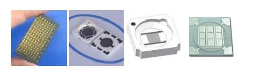
Description
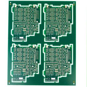
LTCC (Low Temperature Co-fired Ceramic) is a multilayer capable substrate technology offering excellent RF and microwave performance characteristics. Thanks to its low sintering temperature (around 900°C) allows it to co-fire with highly conductive metals such as silver and gold. It is sometimes referred to as “glass ceramics” because glass is mixed in its main raw material, alumina. Elite Advanced Technologies is one of the few LTCC specialists globally that is producing its own green tape (base material low temperature co-fired ceramics). LTCC is best suited for applications that can take advantage of one or more of the following: Good electrical performance Dimensional and electrical stability under temperature, moisture and mechanical stress 3D capability curved, cavities, channels Effective thermal management with metal loaded vias (>100 W/MK) Hermeticity Matched TCE with semiconductors (Thermal Coefficient of Expansion) Multiple assembly and packaging solutions
Product characteristics
- Category
- Thickfilm Thickfilm, LTCC
- Conductor material
- Ag/PdAg Ag/PdAg
- OG (Glass coating)
- Transparent / Black Transparent / Black
- Max # Layers
- 10 10
- Substrate Color
- Grey White, Black
- Panel Size
- 110mmx110mm 120mmx120mm standard (180mmx180mm possible)
- Panel size tolerance
- ±50um ±50um
- Thickness per layer
- 0.25, 0.36 or 0.5mm 0.1, 0.25, 0.38, 0.5, 0.635, 0.8 or 1.0mm
- Thickness tolerance
- ±5% ±5%
- Warpage (non-flatness)
- ≦±0.2% ≦±0.2%
- Warpage
- ≦0.3 %
- Thermal
- ppm/°C Coefficient of Thermal Expansion (CTE)
- Thermal Conductivity
- ≒3 W/MK
Similar products
XIAMEN NINESUN IMP. & EXP. CO., LTD
China

Processing Technology: Electrolytic Foil Base Material: Copper Insulation Materials: Epoxy Resin Certification: UL, RoHS, ISO9001, Ts16949 Transport Package: by Vacuum Packing in Cartons Specification: UL, ROHS, SGS Origin:China HS Code: 85340090 Min. Order: 100 Pieces Port: China Production Capacity:100000 Square Meters Per Month Payment Terms: L/C, T/T, D/P Type: Rigid Circuit Board Dielectric:FR-4 Material: Fiberglass Epoxy Application: Consumer Electronics Flame Retardant Properties: V0 Mechanical Rigid: Rigid
BERATRONIC GMBH
Germany
Our services •Layout creation •Material procurement •SMD assembly •Manual and semi-automatic •Mounting •Reflow and wave soldering •Selective soldering •Automatic Optical Inspection (AOI) •X-ray inspection •System assemblies •In circuit tests and •Function test •Revision and repair •Rework Station •Short delivery times
DAMEKS
Poland
PCB depanelization is a process step in the production of large-scale assembly of electronics. To increase the throughput of printed circuit board (PCB) and surface mount (SMT) production lines, printed circuit boards are often designed to consist of many smaller individual printed circuit boards that will be used in the final product. This PCB cluster is called a panel or multi-block. The large panel is broken or "depanellated" as a process step - depending on the product, this can be right after the SMT process, after the in-circuit test (ICT), after soldering through-hole components, and even just before the final assembly of the PCBA in the enclosure.
DISTRIBUCIONES JULMARSA S.L.
Spain
Designed to meet the needs of smaller, high performance electronic circuitry. These new gap fillers provide an outstanding heat transfer interface across a range of component heights with minimal compression force. THESE PRODUCTS ALL PROVIDE: • Range of thicknesses from 20 mils to 250 mils • Intrinsically tacky surfaces for excellent self-adhesion • Available with various surfaces (no-stick, fabric) for specific application needs • UL 94 V-0 flame retardancy • Large 24" x 24" sheet sizes for improved die-cutting yield with custom sizes available • Range of compliance and thermal conductivities to fit specific applications
Request for quotes
Create one request and get multiple quotes form verified suppliers.
- Only relevant suppliers
- Data privacy compliant
- 100% free