Rigid-Flex PCB
Description
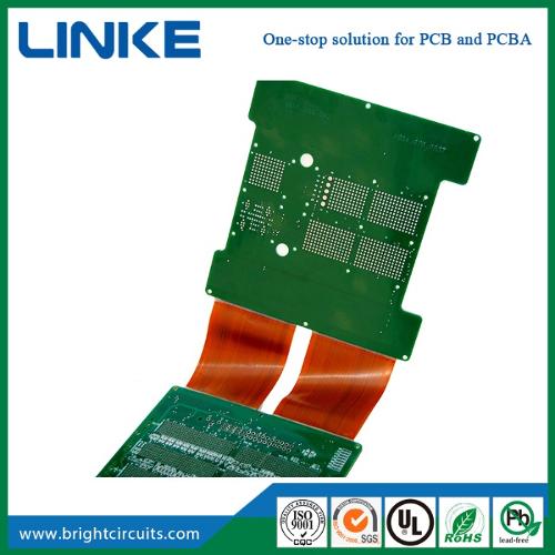
The rigid-flex PCB is a flexible PCB circuit board and a rigid PCB circuit board, which are combined together according to the relevant process requirements through the pressing and other processes to form a circuit board with Flex PCB and Rigid PCB characteristics.
- Printed circuits
- Rigid-Flex PCB
- Rigid Flex PCB
- double side pcb
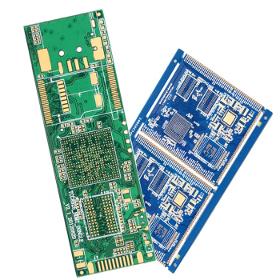
Similar products
XIAMEN NINESUN IMP. & EXP. CO., LTD
China

Place of Origin: China Base Material: FR-4 Copper Thickness: 1/2OZ 1OZ 2OZ 3OZ Board Thickness: 0.8mm Min. Hole Size: 0.1mm Min. Line Width: 0.065mm Min. Line Spacing: 0.065mm Surface Finishing: HASL Application: Electronics Device Type: Customizable Solder mask: Black Material: FR4 CEM1 CEM3 height TG Color: Red Blue Green Black Testing Service: 100% Supply Ability: 25000 Square Meter/Square Meters per Month

BERATRONIC GMBH
Germany
Technical data •Max. Panel size up to 1500mm x 670mm •PCB thickness from 0.1-17.5mm •Smallest hole 0.075mm •Smallest trace/spacing 50µm •Copper layer up to 1000µm •Number of layers up to 58 •Aspect Ratio 20:1 •Rigid flex and flex •Viaplugging •Impedance control •Laser Microvias •Blind, Buried Vias Basic material •FR4, FR4 High TG, FR4 •halogen-free, CEM1/3, Rogers, •Ceramic (Al2O3), polyimide and others Surface •HAL lead-free, HAL Pb/Sn, chem. Ni/Au (ENIG), chem. Ni/Pd/Au (ENEPIG), chem. Sn, chem. Ag, OSP(Entek), galv. Ni/Au, Carbon, Ag/Pt (thick film technology) and others Solder resist and placement printing •Different paint systems (including halogen-free) and colors Standards •ISO 9001:2015 / IATF 16949 •UL listing •RoHS / REACH •Manufacturing according to IPC A600 class 2 and 3 Delivery times •Rush service from 1 AT •Series from 10 AT Data preparation •Legacy document preparation •Scan Service •Data conversion •CAM data preparation •CAD layout service
DAMEKS
Poland
PCB depanelization is a process step in the production of large-scale assembly of electronics. To increase the throughput of printed circuit board (PCB) and surface mount (SMT) production lines, printed circuit boards are often designed to consist of many smaller individual printed circuit boards that will be used in the final product. This PCB cluster is called a panel or multi-block. The large panel is broken or "depanellated" as a process step - depending on the product, this can be right after the SMT process, after the in-circuit test (ICT), after soldering through-hole components, and even just before the final assembly of the PCBA in the enclosure.
DISTRIBUCIONES JULMARSA S.L.
Spain
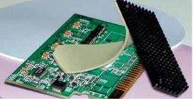
Designed to meet the needs of smaller, high performance electronic circuitry. These new gap fillers provide an outstanding heat transfer interface across a range of component heights with minimal compression force. THESE PRODUCTS ALL PROVIDE: • Range of thicknesses from 20 mils to 250 mils • Intrinsically tacky surfaces for excellent self-adhesion • Available with various surfaces (no-stick, fabric) for specific application needs • UL 94 V-0 flame retardancy • Large 24" x 24" sheet sizes for improved die-cutting yield with custom sizes available • Range of compliance and thermal conductivities to fit specific applications
Request for quotes
Create one request and get multiple quotes form verified suppliers.
- Only relevant suppliers
- Data privacy compliant
- 100% free