Electron Microscopy
Nanomanipulator OmniProbe 400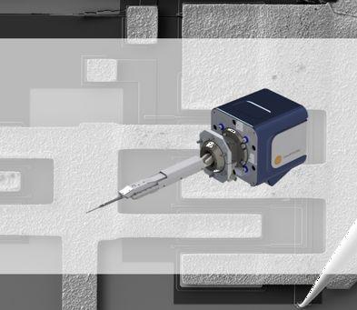
Description
A ninth generation of nanomanipulator, the OmniProbe 400 exploits innovative piezo actuation for best in class nanoscale positioning. Optimised for maximum flexibility and performance, the OmniProbe 400 is the ultimate nanomanipulator for high resolution and high throughput applications. - 4_3 performance Nanoscale manipulation and testing in the SEM and varied lift-out TEM sample preparations in the FIB can be performed easily while using optimized working distances - 4 degrees of freedom (X, Y, Z, R), - 4 mm or more working distance, - 4 motion strengths: encoder resolution, motor resolution, repeatability, linearity. ** Click to request pricing **
- Scientific research equipment
- Nanoanalysis
- Nanomanipulator
- electron microscopy
Similar products
SHENZHEN PROMOSTAR HARDWARE CO.,LTD
Germany

New craft 6: Environmentally friendly electroless nickel plating. Nickel plating in strict accordance with customer requirements,we can control the accurate thickness.
KNIGHT OPTICAL (UK) LTD
United Kingdom
When it comes to a high quality IR Cut filter, it is the substrate with the coating applied that affects the performance. Knight Optical provide high quality wafers for precisely this, and the surface quality of our substrates eliminates blotching at the sensor which occurs on lower quality substrates especially where IR Cut filters are concerned. Our wafers are produced as thin as 500μm & provide exceptional surface quality. However, we can manufacture to a fully customised specification with a wafer thickness as little as 10 μm. Our substrates for stock or custom can be manufactured from a great deal of materials including: •Quartz •Borosilicate •BK7 or equivalent •Sapphire •And many more. Depending on your application for the IR Cut Filter, we can help advise on the best achievable optic for your application. Please read PDF for full specification

SCHNIEWINDT GMBH & CO. KG
Germany
We carry out applied research in our own test field and laboratory in order to constantly further develop our products, but also so as to be able to present our customers with innovative new developments. Furthermore, we regularly participate in cooperative projects of the Federal PhysicalTechnical Institute (PTB PhysikalischTechnische Bundesanstalt) with the economy. We also maintain close cooperative links with the universities of DuisburgEssen and Karlsruhe. We would also like to support you in research with our products. Please contact us.

CRB ANALYSE SERVICE GMBH
Germany
The application possibilities of the scanning electron microscope, SEM in combination with the energy dispersive X-ray microanalysis, EDX are manifold. The areas of application listed here are only examples of some of the applications. Many other questions can be clarified with our microtextural and microanalytical test methods. Our services for you: X-ray microanalysis, EDX element mappings, line scans, SEM imaging, particle size determination, fiber thickness measurement, damage assessment
Request for quotes
Create one request and get multiple quotes form verified suppliers.
- Only relevant suppliers
- Data privacy compliant
- 100% free