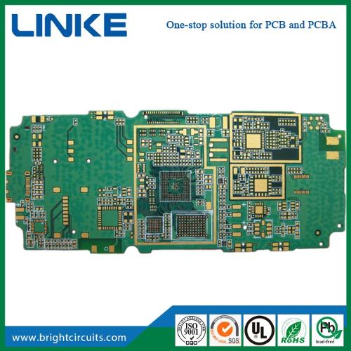
Immersion Gold PCB
Description
Simply put, Immersion Gold PCB uses a chemical deposition method to produce a layer of metal plating on the surface of the circuit board through chemical redox reactions.
- Printed circuits
- PCB Prototype
- double side pcb
- PCB board
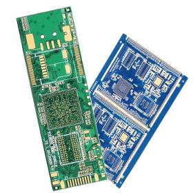
Similar products
XIAMEN NINESUN IMP. & EXP. CO., LTD
China

Place of Origin: China Base Material: FR-4 Copper Thickness: 1/2OZ 1OZ 2OZ 3OZ Board Thickness: 0.8mm Min. Hole Size: 0.1mm Min. Line Width: 0.065mm Min. Line Spacing: 0.065mm Surface Finishing: HASL Application: Electronics Device Type: Customizable Solder mask: Black Material: FR4 CEM1 CEM3 height TG Color: Red Blue Green Black Testing Service: 100% Supply Ability: 25000 Square Meter/Square Meters per Month
DAMEKS
Poland
PCB depanelization is a process step in the production of large-scale assembly of electronics. To increase the throughput of printed circuit board (PCB) and surface mount (SMT) production lines, printed circuit boards are often designed to consist of many smaller individual printed circuit boards that will be used in the final product. This PCB cluster is called a panel or multi-block. The large panel is broken or "depanellated" as a process step - depending on the product, this can be right after the SMT process, after the in-circuit test (ICT), after soldering through-hole components, and even just before the final assembly of the PCBA in the enclosure.
SEACOMP
United States
SEACOMP Engineering and Design for Manufacturing (DFM) Enhance your product with our design engineering and design for manufacturing (DFM) services. We'll review your product design and ensure it meets your functional requirements and give any recommendations on how to best meet your product goals. Your product design will also be prepped so that it is ready for manufacturing. All of our design engineering services are completed in-house at our U.S. headquarters.

BERATRONIC GMBH
Germany
Technical data •Max. Panel size up to 1500mm x 670mm •PCB thickness from 0.1-17.5mm •Smallest hole 0.075mm •Smallest trace/spacing 50µm •Copper layer up to 1000µm •Number of layers up to 58 •Aspect Ratio 20:1 •Rigid flex and flex •Viaplugging •Impedance control •Laser Microvias •Blind, Buried Vias Basic material •FR4, FR4 High TG, FR4 •halogen-free, CEM1/3, Rogers, •Ceramic (Al2O3), polyimide and others Surface •HAL lead-free, HAL Pb/Sn, chem. Ni/Au (ENIG), chem. Ni/Pd/Au (ENEPIG), chem. Sn, chem. Ag, OSP(Entek), galv. Ni/Au, Carbon, Ag/Pt (thick film technology) and others Solder resist and placement printing •Different paint systems (including halogen-free) and colors Standards •ISO 9001:2015 / IATF 16949 •UL listing •RoHS / REACH •Manufacturing according to IPC A600 class 2 and 3 Delivery times •Rush service from 1 AT •Series from 10 AT Data preparation •Legacy document preparation •Scan Service •Data conversion •CAM data preparation •CAD layout service
Request for quotes
Create one request and get multiple quotes form verified suppliers.
- Only relevant suppliers
- Data privacy compliant
- 100% free