
SAND TECH CO.
Egypt
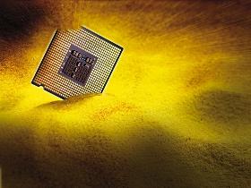
Silicon is the most common semiconductor and the most widely used in the electronic and technology sector. There are different silicon fabrication methods including the horizontal gradient freeze method and vertical Bridgeman method. Silicon is the principal platform for a semiconductor device, a wafer is a thin slice of this semiconductor material, which serves as the substrate for a microelectronic device built in and over the wafer. Silicon wafer’s primary use in integrated circuits which power many of the products that modern society uses every day. Computers, smartphones and solar cells are only three products that are dependent on this technology. although other semiconductors have been tested over time, silicon has proved to be a stable option.
XIAMEN NINESUN IMP. & EXP. CO., LTD
China

Product name: 2-12 Inch Orientation 100/111/110 SSP Prime/Dummy Grade Silicon Wafer Place of Origin: China Material: Silicon Diameter:2-12 inch Thickness: 100-1500um Orientation: 100/110/111 Type/Dopant: intrinsic or P/B or N/Ph Grade: prime/dummy Bow/Warp:<30um TTV:<10um Surface finish: SSP/DSP Supply Ability: 20000 Piece/Pieces per Month Packaging Details:Stardand Package Port of shipment: Xiamen,China Lead Time :25-30days
KNIGHT OPTICAL (UK) LTD
United Kingdom
Germanium wafers are a semiconductor material & therefore are a smart choice for microelectronics. Due to its unique electric properties, it is widely used for sensors, solar cells and infrared optical applications. The wafers are also great for microelectronics as the space is limited and being available in 500μm or less it makes it perfect to achieve the high quality results required. It’s thermal conductivity makes it a good alternative to silicon. Our stock wafers are produced as thin as 500μm and provide exceptional surface quality. However, we can manufacture to a fully customised specification with a wafer thickness as little as 10 μm. Typical specifications of our germanium wafers are: 10mm – 150mm in diameter <500μm in thickness Doped and undoped Germanium
PEEKCHINA CO., LTD.
China
Size: 4", 5", 6", 8", 12" & Non Standard. PEEK handheld tool, a tool for handheld inspection of wafers. PEEK does not contain halogen elements and does not contaminate semiconductor wafers.

Do you sell or make similar products?
Sign up to europages and have your products listed
N&H TECHNOLOGY GMBH
Germany
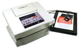
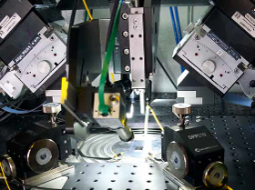
The Loresta GX is used to measure conductors and semiconductors in the lower resistance range. Measuring range: 10^-4 – 10^7 Ω. It is used to measure the surface resistivity (Ω / □), the volume resistivity (Ω · cm), electrical conductivity (S / cm) in the low-resistance range. The Loresta-GX works according to the 4-pin measuring method. The method is based on the four-wire method and was developed to eliminate the influence of contact resistance. The measuring heads consist of four needle-like electrodes. To simplify the measurement method and calculate the correction factors, all four electrodes are at an equidistant distance from each other. Conductive Materials: Paints, pastes, paints, printing ink, Smart Textiles, Plastics, rubber Film materials, metallic thin films, metallised films, resistor pastes amorphous silicon / silicon wafer, antistatic materials, EMC shielding materials ...
INFICON GMBH
Germany
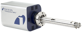
UNLOCK YOUR PROCESS Unparalleled Performance for Increased Yields and Maximum Uptime The ever increasing price of silicon wafers and demand for finished products means that scrapped wafers cost more than ever before. Thus, understanding your process and monitoring for defects has become a much higher priority in semiconductor fabrication centers. The Transpector MPH Gas Analysis System is designed to unlock your process with industry leading performance for all of your gas analysis applications to help maximize chip yields and minimize tool downtime. Combined with a low overall cost of ownership and high mean-time-between-failures, Transpector MPH helps your bottom line more than any other residual gas analyzer (RGA) on the market. INFICON has leveraged its expertise in gas analysis process control equipment to create an RGA with industry-leading data collection speed, minimum detectable partial pressure and signal-to-noise ratio. All this, without sacrificing any of the...
XIAMEN INNOVACERA ADVANCED MATERIALS CO., LTD
China
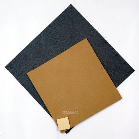
Innovacera uses its deep ceramics expertise and process capabilities to manufacture ceramics with precisely controlled porosity. Porous ceramics are often used for chemical filtration and fluid separation. The range of Innovacera porous ceramics is made from aluminum oxide and silicon carbide. The strong, uniform porous ceramic has 40-50% open porosity with a tortuous pore structure and is available in pore sizes ranging from 1 to 100 microns. Three Main Application of Porous Ceramic: Vacuum Chuck, like scribing machine vacuum chuck, silicon wafer vacuum chuck. Adsorption platform. Suspension platform. Especially, they are widely used for the semiconductor industry, like LED wafer processing. The micro-porous ceramic working disk is a special tool for adsorption and bearing in various semiconductor wafer production processes, and is applied to processes such as thinning, dicing, cleaning, and handling.
NANOSYSTEC GMBH
Germany
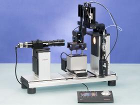
All NanoTest stations combines precise measurements with high speed, proven reliability and ease of use. The versatility qualifies the stations not only for high volume quality assurance, but also for demanding development applications. This qualification helps to differentiate well-working devices from the ones with mediocre performance. In this way, unnecessary processing of low-quality devices is avoided early and possible problems during wafer production will be determined. NanoTest-W characterizes the optical and electrical behavior of VCSEL or Silicon Photonics chips on wafer level, while NanoTest-C is used for laser diodes, receivers and passive devices on bar or chip level.
NANJING LAB
United Kingdom
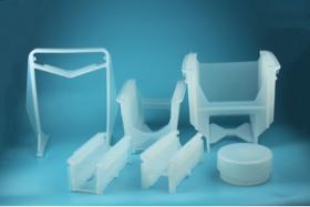
There are many types of wafer carriers, and each has its own application. For example, the front-opening wafer transfer box FOUP can be used in the semiconductor process in the manufacturing plant, the front-opening wafer transport box FOSB can be used for transportation between manufacturing plants, and the wafer flower basket can be used. for wafer cleaning, etc. Fluororesin has an extremely stable molecular structure, so it is hardly affected by light, temperature and chemicals, and is the "king of resins" that subverts the inherent concept. In the process of cleaning chips, high-purity chemicals are required, and fluoropolymers are the only materials that can contain and transport the high-purity chemicals used in the manufacturing process, achieving the extremely high stability and purity required for semiconductor manufacturing.
DATAPHYSICS INSTRUMENTS GMBH
Germany
The optical contact angle meters of the OCA series are high-precision measuring systems for the characterisation of interfaces and surfaces. They combine high-resolution optics, pinpoint liquid dosing and precise sample positioning to create powerful, reliable measuring systems. The expert model OCA 200 is the contact angle measuring instrument for microscopic and macroscopic structures. Thanks to the 10x zoom lens and the autofocus system, the OCA 200 is suitable for any sample size from the macroscopic silicon wafer to the microscopic metal struts of a coronary stent. Together with the PDDS picolitre dosing system, the OCA 200 allows the analysis of droplets with a minimum volume of up to 30 picolitres. Measurements: - static contact angle - dynamic contact angle - interfacial and surface tension - surface energy - viscoelastic modulus - work of adhesion

PRECISION SURFACING SOLUTIONS GMBH & CO. KG
Germany
The Peter Wolters AC 2000 double-sided batch processing machine is designed for high-precision series production of workpieces. Thanks to its modular design, the AC 2000 can be used as a fine grinding, lapping, honing and polishing machine. Like all machines in the microLine© series, the AC 2000 relies on proven core components such as the high-precision pneumatic loading system, the non-contact micro-measurement control, the powerful drive technology and the PC-supported machine guidance. The software used for this is specially developed by Peter Wolters and enables complete menu-driven and intuitive operation of the machine. For optimum access to the working area, the entire upper part of the machine can be swung out.
Results for
Silicon wafer - Import exportNumber of results
13 ProductsCountries
Company type
Category