WIN WIN CIRCUIT LTD.
China
Manufacturer/ Producer
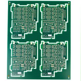
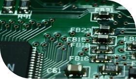
Win Win Circuit LTD., located in Zhuhai and Macao, is a multicultural enterprise focus on high-tech electronic component: PCB and PCBA, LCD Module, LED LightingPCB: the pioneer department of company which has a team with decade year’s experiences in this industry.PCB Dept. provide you with quicker and profession services.Our factory includes the eighth PCB factory in the world.PCBA: Founded in July of 1997Total floor space: 40000㎡. Main Operation: PCBA(SMT, COB, DIP, COG) and final product assembly manufacturing.Main product: Consumer products, Touch Screen, medical products, automotive products, industrial meter and other high accuracy electronic products.Managing system certificate: ISO 14001, ISO 9001, ISO/TS 16949LCD Module: TFT Module, LCM, LCD Panel, Digital Touch Screen, Resistive Touch Screen, Capacitive Touch Screen, Touch Lens, Surface Acoustic WaveLED Lighting: LED Tube, LED Strip, LED Star, LED Bulb, LED Streetlight, LED Downlight, LED Ceiling Lamp
Website
Manufacturer/ Producer
802,2u,18b,rongtaiheting
519000 Zhuhai - China
Company info
Key figures
-
- Company headcount
- > 500
-
- Sales staff
- 11 – 50
-
- % of export sales
- 100%
Organisation
-
- Year established
- 1997
-
- pages.epage-home.site-status
- Registered office
-
- Main activity
- Manufacturer/ Producer
Business info
Trading areas
- European
- International
Payment methods
- Telex transfer
Delivery areas
Activities of WIN WIN CIRCUIT LTD.
- Printed circuits
- Printed circuit board relays
- PCBA
europages also recommends
A selection of companies related to the activity:
A selection of products that might interest you
XIAMEN NINESUN IMP. & EXP. CO., LTD
China

Processing Technology: Electrolytic Foil Base Material: Copper Insulation Materials: Epoxy Resin Certification: UL, RoHS, ISO9001, Ts16949 Transport Package: by Vacuum Packing in Cartons Specification: UL, ROHS, SGS Origin:China HS Code: 85340090 Min. Order: 100 Pieces Port: China Production Capacity:100000 Square Meters Per Month Payment Terms: L/C, T/T, D/P Type: Rigid Circuit Board Dielectric:FR-4 Material: Fiberglass Epoxy Application: Consumer Electronics Flame Retardant Properties: V0 Mechanical Rigid: Rigid

BERATRONIC GMBH
Germany
Our services •Layout creation •Material procurement •SMD assembly •Manual and semi-automatic •Mounting •Reflow and wave soldering •Selective soldering •Automatic Optical Inspection (AOI) •X-ray inspection •System assemblies •In circuit tests and •Function test •Revision and repair •Rework Station •Short delivery times

BERATRONIC GMBH
Germany
Technical data •Max. Panel size up to 1500mm x 670mm •PCB thickness from 0.1-17.5mm •Smallest hole 0.075mm •Smallest trace/spacing 50µm •Copper layer up to 1000µm •Number of layers up to 58 •Aspect Ratio 20:1 •Rigid flex and flex •Viaplugging •Impedance control •Laser Microvias •Blind, Buried Vias Basic material •FR4, FR4 High TG, FR4 •halogen-free, CEM1/3, Rogers, •Ceramic (Al2O3), polyimide and others Surface •HAL lead-free, HAL Pb/Sn, chem. Ni/Au (ENIG), chem. Ni/Pd/Au (ENEPIG), chem. Sn, chem. Ag, OSP(Entek), galv. Ni/Au, Carbon, Ag/Pt (thick film technology) and others Solder resist and placement printing •Different paint systems (including halogen-free) and colors Standards •ISO 9001:2015 / IATF 16949 •UL listing •RoHS / REACH •Manufacturing according to IPC A600 class 2 and 3 Delivery times •Rush service from 1 AT •Series from 10 AT Data preparation •Legacy document preparation •Scan Service •Data conversion •CAM data preparation •CAD layout service
DAMEKS
Poland
PCB depanelization is a process step in the production of large-scale assembly of electronics. To increase the throughput of printed circuit board (PCB) and surface mount (SMT) production lines, printed circuit boards are often designed to consist of many smaller individual printed circuit boards that will be used in the final product. This PCB cluster is called a panel or multi-block. The large panel is broken or "depanellated" as a process step - depending on the product, this can be right after the SMT process, after the in-circuit test (ICT), after soldering through-hole components, and even just before the final assembly of the PCBA in the enclosure.
Request for quotes
Create one request and get multiple quotes form verified suppliers.
- Only relevant suppliers
- Data privacy compliant
- 100% free