FERROTEC CHINA
China
Manufacturer/ Producer
Direct bonded copper (DBC) substrates consist of a ceramic isolator, Al2O3 (aluminium oxide) or AlN (aluminium nitride), to which pure copper is applied in a high temperature melting and diffusion process. The result is a non-detachable connection of copper and ceramics. Due to the high heat conductivity of Al2O3 (24 W/mK) and AlN (130 to 180 W/mK) and the excellent heat capacity of the thick copper coating (200 - 600 μm) DBC substrates are ideally suited for high power electronics. The temperature coefficient of expansion (TCE) of Al2O3 and AlN closely matches that of silicon. This minimizes the mechanical stress in the bare silicon die which is attached to the substrate since the TCE of DBC Al2O3 and AlN are much closer to that of silicon than other materials.
Website
Manufacturer/ Producer
No.181 Shanlian Rd. Baoshan Urban Industrial Garden, Shanghai, P.R.China
201900 Shanghai - China
Company info
Key figures
-
- Company headcount
- > 500
Organisation
-
- Main activity
- Manufacturer/ Producer
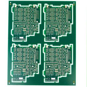
Activities of FERROTEC CHINA
- Printed circuits
- DBC Substrate
- Metallized Ceramic
europages also recommends
A selection of companies related to the activity:
A selection of products that might interest you
XIAMEN NINESUN IMP. & EXP. CO., LTD
China

Processing Technology: Electrolytic Foil Base Material: Copper Insulation Materials: Epoxy Resin Certification: UL, RoHS, ISO9001, Ts16949 Transport Package: by Vacuum Packing in Cartons Specification: UL, ROHS, SGS Origin:China HS Code: 85340090 Min. Order: 100 Pieces Port: China Production Capacity:100000 Square Meters Per Month Payment Terms: L/C, T/T, D/P Type: Rigid Circuit Board Dielectric:FR-4 Material: Fiberglass Epoxy Application: Consumer Electronics Flame Retardant Properties: V0 Mechanical Rigid: Rigid
BERATRONIC GMBH
Germany
Our services •Layout creation •Material procurement •SMD assembly •Manual and semi-automatic •Mounting •Reflow and wave soldering •Selective soldering •Automatic Optical Inspection (AOI) •X-ray inspection •System assemblies •In circuit tests and •Function test •Revision and repair •Rework Station •Short delivery times
BERATRONIC GMBH
Germany
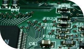
Technical data •Max. Panel size up to 1500mm x 670mm •PCB thickness from 0.1-17.5mm •Smallest hole 0.075mm •Smallest trace/spacing 50µm •Copper layer up to 1000µm •Number of layers up to 58 •Aspect Ratio 20:1 •Rigid flex and flex •Viaplugging •Impedance control •Laser Microvias •Blind, Buried Vias Basic material •FR4, FR4 High TG, FR4 •halogen-free, CEM1/3, Rogers, •Ceramic (Al2O3), polyimide and others Surface •HAL lead-free, HAL Pb/Sn, chem. Ni/Au (ENIG), chem. Ni/Pd/Au (ENEPIG), chem. Sn, chem. Ag, OSP(Entek), galv. Ni/Au, Carbon, Ag/Pt (thick film technology) and others Solder resist and placement printing •Different paint systems (including halogen-free) and colors Standards •ISO 9001:2015 / IATF 16949 •UL listing •RoHS / REACH •Manufacturing according to IPC A600 class 2 and 3 Delivery times •Rush service from 1 AT •Series from 10 AT Data preparation •Legacy document preparation •Scan Service •Data conversion •CAM data preparation •CAD layout service
DAMEKS
Poland
PCB depanelization is a process step in the production of large-scale assembly of electronics. To increase the throughput of printed circuit board (PCB) and surface mount (SMT) production lines, printed circuit boards are often designed to consist of many smaller individual printed circuit boards that will be used in the final product. This PCB cluster is called a panel or multi-block. The large panel is broken or "depanellated" as a process step - depending on the product, this can be right after the SMT process, after the in-circuit test (ICT), after soldering through-hole components, and even just before the final assembly of the PCBA in the enclosure.
Request for quotes
Create one request and get multiple quotes form verified suppliers.
- Only relevant suppliers
- Data privacy compliant
- 100% free