NANOSYSTEC GMBH
Germany
Manufacturer/ Producer
NANOSYSTEC GMBH
Germany
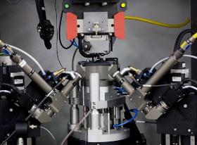
The fine balancing system NanoBalancer corrects smallest imbalances of rotating work pieces with laser ablation. The removal of material is performed either statically after the measurement or dynamically during the rotation of the work piece. Typical examples are impellers for technical or medical applications, airdriven turbines or small rotors of miniature motors.
NANOSYSTEC GMBH
Germany
The work area of 700 x 900 mm offers sufficient space. The motion system works with linear motors and linear optical encoders which guarantee extremely high resolution and precision – even at the high speed due to the excellent acceleration of the linear motors. The empty surface of the vertical stage is equipped with an interface for fast tool changing. Sensors measure the force applied by the tools to the device. The desired forces can be programmed so that each device is handled ideally.Eutectic bonding is performed with high energy laser radiation and with a wavelength matched to the device. Temperature sensors transmit the values to the control electronics and the power is precisely adapted. In this way, the temperature follows the desired profile fast and accurately. NanoBond utilizes precision dispensers for gluing processes. These instruments apply a volume from nanoliters to several milliliters. In most application
NANOSYSTEC GMBH
Germany
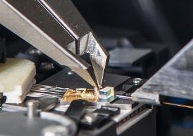
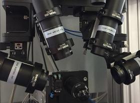
NanoGlue serves as the ideal assembly station for opto-electronic components, such as photonics circuits,waveguides, diode lasers and photodiodes as well as lenses and modulators. It provides active alignment in all six degrees of freedom followed by epoxy gluing with UV curing.
NANOSYSTEC GMBH
Germany
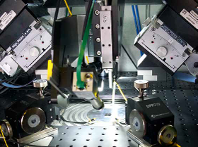
NanoHybrid provides a large degree of versatility. The active alignment, test and assembly station combines various assembly methods including gluing, laser welding or selective laser soldering. In addition, the station offers opto-electronic testing capability. Therefore, NanoHybrid is ideally suited for the development and small serial production in manufacturing companies or in research institutes. In such a product development area, an active alignment station needs to cope with opto-electronic and other precision devices with varying sizes and characteristics.
NANOSYSTEC GMBH
Germany
NanoSolder actively aligns optical components such as photonic circuits, waveguides, diode lasers and photodiodes. It uses selective laser soldering for the assembly. Compared to gluing with subsequent curing, much shorter assembly times will be achieved by selective laser soldering.
NANOSYSTEC GMBH
Germany
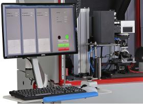
Reliable Opto-Electronic Characterization for DC and RF Values The opto-electronic test station NanoTest PIC HD complies with all requirements for the testing of high-density photonics integrated circuits, such as silicon photonics structures or active PICs. Probe cards with up to several hundreds of contacts provide the connection for DC and RF measurements.
NANOSYSTEC GMBH
Germany
All NanoTest stations combines precise measurements with high speed, proven reliability and ease of use. The versatility qualifies the stations not only for high volume quality assurance, but also for demanding development applications. This qualification helps to differentiate well-working devices from the ones with mediocre performance. In this way, unnecessary processing of low-quality devices is avoided early and possible problems during wafer production will be determined. NanoTest-W characterizes the optical and electrical behavior of VCSEL or Silicon Photonics chips on wafer level, while NanoTest-C is used for laser diodes, receivers and passive devices on bar or chip level.
NANOSYSTEC GMBH
Germany
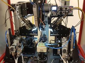
NanoTest VCSEL measures VCSEL on wafer level or Chip on Carrier regarding their optical and electrical characteristics. The tester accommodates wafers with a diameter of up to 6 inches (150 mm), as an option also larger diameters can be integrated. A special interface mounted to the chuck also allows for testing Chip on Carrier devices.A high-precision motion system with XYZ and rotary adjustment brings the wafer chuck in the respective measurement position. First, electrical contacting takes place supported by a sideview camera. A high-precision current source delivers the operating current for the VCSEL under test.
NANOSYSTEC GMBH
Germany
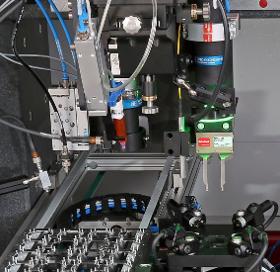
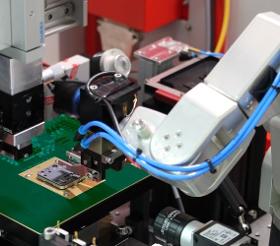
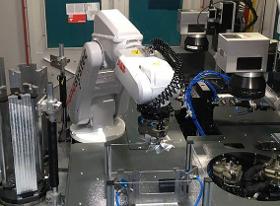
The NanoWeld stations provide the ideal platform for the development and production of opto-electronic components, like singleand multi-channel transmitters and receivers. The station works with exchangeable trays and grippers accepting all device housing types and lenses, optical fibers or receptacles to be aligned and attached. Cycle times for the rapid mass production of TOSA type assemblies reach less than 25 seconds while it takes several minutes for complex devices.All components and subassemblies to build the NanoWeld station are of highest quality and performance. Even customized systems start from a common platform which minimizes development time and cost. By using device-specific trays and grippers, the time to change between different batch processes or device types is reduced to the minimum. Loading and unloading of these trays is performed on a separate loading station outside of the automated NanoWeld. The automated alignment starts from a known reference position.
NANOSYSTEC GMBH
Germany
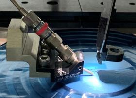
The laser processing station VersaCut precisely ablates and cuts a large variety of materials, such as metals (stainless steel, nonferrous metals), ceramics like Si or AlN, and all kind of plastics. Depending on the indented use, the station uses different laser sources with the corresponding focusing optics. The modular VersaCut finds it application in research and production.A solid-state laser delivering short pulses in the nanosecond regime is ideal for cutting stainless steel, Kovar, brass and similar metals. The high peak power with a small focus on the target generates the necessary power density for clean and sharp cuts. There is however an impact on the surrounding area as some local heating occurs. The high peak power allows also for cutting and ablating plastics, even if the laser wavelength does not match the linear absorption of the plastic.
Manufacturer/ Producer
Marie-Curie-Strasse 6
64823 Gross-Umstadt - Germany
europages also recommends
A selection of companies related to the activity:
A selection of products that might interest you

GEMONE
Belgium

This service includes connection to any type of machine, integration with your current hardware and software, providing end-user training during onboarding, and swiftly and securely handle your data in the Cloud. This allows you to concentrate entirely on your business.
GEMONE
Belgium
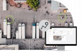
Stay informed about the precise location of your machines at all times, whether they're inside your facility, on your premises, or in transit. Each machine is equipped with a durable tracker that maintains continuous communication with the GemOne platform.

AIS HENSCH AUTOMATION-INDUSTRY- SOLUTIONS INH. IGOR HENSCH
Germany
The industrial CPUs from AIS Hensch Automation-Industry-Solution represent a first-class solution for controlling automated production processes in various industrial sectors. These CPUs are characterized by their technological excellence, reliability and versatility, making them an indispensable component for optimizing manufacturing processes. Thanks to their powerful processing, our industrial CPUs offer precise control that can be seamlessly integrated into a wide variety of production environments. From the oil and gas industry to mechanical engineering, these CPUs flexibly adapt to the specific requirements of different industries. The robustness and longevity of our industrial CPUs ensure reliable performance even under demanding conditions.
Request for quotes
Create one request and get multiple quotes form verified suppliers.
- Only relevant suppliers
- Data privacy compliant
- 100% free