SET PCB TECHNOLOGY LTD.
Bulgaria
Manufacturer/ Producer
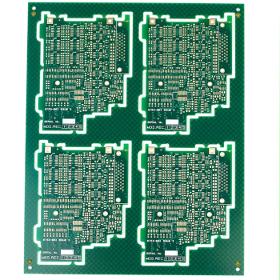
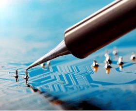
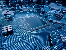
SET PCB Technology is a professional electronic manufacturer offering: Low prices, High quality and Fast delivery. With the extensive expertise of our engineers we are concentrated on complete service starting from a fast offer to a professional flexible production. As a result the customers get cheap electronics in highest quality. As an innovative and dynamic market-driven company SET PCB Technology is specialised in providing high quality tested PCBs and electronic assembly. We are specialised in the production of single-sided, double-sided and multi-layer PCBs of different shape and size in compliance with customer’s specifications and requirements.The company also manufactures some special PCBs as MS Aluminium PCBs, High Frequency PCBs, Flexible PCBs, High-Tg PCBs, Thick-copper PCBs up to 400 µm. SET produces in Ruse, Bulgaria with currently around 150 employees. We manufacture printed circuit board prototypes and serial production in standard and express service.
Website
Manufacturer/ Producer
1 Blvd. Hristo Botev, BG-7018 Ruse, Bulgaria
7018 Ruse - Bulgaria
Company info
Key figures
-
- Company headcount
- 101 – 200
Organisation
-
- Year established
- 1969
-
- Main activity
- Manufacturer/ Producer
Business info
Trading areas
- European
Delivery areas
Activities of SET PCB TECHNOLOGY LTD.
- Printed circuits
- PCBs
- electronic manufacturer
- leiterplatten
- PCB prototypes
europages also recommends
A selection of companies related to the activity:
A selection of products that might interest you
XIAMEN NINESUN IMP. & EXP. CO., LTD
China

Processing Technology: Electrolytic Foil Base Material: Copper Insulation Materials: Epoxy Resin Certification: UL, RoHS, ISO9001, Ts16949 Transport Package: by Vacuum Packing in Cartons Specification: UL, ROHS, SGS Origin:China HS Code: 85340090 Min. Order: 100 Pieces Port: China Production Capacity:100000 Square Meters Per Month Payment Terms: L/C, T/T, D/P Type: Rigid Circuit Board Dielectric:FR-4 Material: Fiberglass Epoxy Application: Consumer Electronics Flame Retardant Properties: V0 Mechanical Rigid: Rigid
BERATRONIC GMBH
Germany
Our services •Layout creation •Material procurement •SMD assembly •Manual and semi-automatic •Mounting •Reflow and wave soldering •Selective soldering •Automatic Optical Inspection (AOI) •X-ray inspection •System assemblies •In circuit tests and •Function test •Revision and repair •Rework Station •Short delivery times
BERATRONIC GMBH
Germany
Technical data •Max. Panel size up to 1500mm x 670mm •PCB thickness from 0.1-17.5mm •Smallest hole 0.075mm •Smallest trace/spacing 50µm •Copper layer up to 1000µm •Number of layers up to 58 •Aspect Ratio 20:1 •Rigid flex and flex •Viaplugging •Impedance control •Laser Microvias •Blind, Buried Vias Basic material •FR4, FR4 High TG, FR4 •halogen-free, CEM1/3, Rogers, •Ceramic (Al2O3), polyimide and others Surface •HAL lead-free, HAL Pb/Sn, chem. Ni/Au (ENIG), chem. Ni/Pd/Au (ENEPIG), chem. Sn, chem. Ag, OSP(Entek), galv. Ni/Au, Carbon, Ag/Pt (thick film technology) and others Solder resist and placement printing •Different paint systems (including halogen-free) and colors Standards •ISO 9001:2015 / IATF 16949 •UL listing •RoHS / REACH •Manufacturing according to IPC A600 class 2 and 3 Delivery times •Rush service from 1 AT •Series from 10 AT Data preparation •Legacy document preparation •Scan Service •Data conversion •CAM data preparation •CAD layout service

Request for quotes
Create one request and get multiple quotes form verified suppliers.
- Only relevant suppliers
- Data privacy compliant
- 100% free