Product launch
・ 11 May 2017
- 31 Dec 2017
・
read more
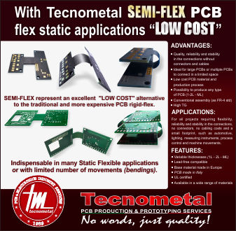
SEMI-FLEX represent an excellent "LOW COST" alternative to the traditional and more expensive PCB rigid-flex. Indispensable in many Static Flexible applications or with limited number of movements (bendings). ADVANTAGES: Quality, reliability and stability in the connections without connectors and cables - Ideal for large PCBs or multiple PCBs to connect in a limited space - Low cost PCB material and production process - Possibility to produce any type of PCB (1-2L - ML) - Conventional assembly (as FR-4 std) - High TG
TECNOMETAL - NEW WEBSITE
Latest project
・ 26 Sept 2016
- 14 Oct 2016
We published our new website at www.tecnometal.net
Technical data
•Max. Panel size up to 1500mm x 670mm
•PCB thickness from 0.1-17.5mm
•Smallest hole 0.075mm
•Smallest trace/spacing 50µm
•Copper layer up to 1000µm
•Number of layers up to 58
•Aspect Ratio 20:1
•Rigid flex and flex
•Viaplugging
•Impedance control
•Laser Microvias
•Blind, Buried Vias
Basic material
•FR4, FR4 High TG, FR4
•halogen-free, CEM1/3, Rogers,
•Ceramic (Al2O3), polyimide and others
Surface
•HAL lead-free, HAL Pb/Sn, chem. Ni/Au (ENIG), chem. Ni/Pd/Au (ENEPIG), chem. Sn, chem. Ag, OSP(Entek), galv. Ni/Au, Carbon, Ag/Pt (thick film technology) and others
Solder resist and placement printing
•Different paint systems (including halogen-free) and colors
Standards
•ISO 9001:2015 / IATF 16949
•UL listing
•RoHS / REACH
•Manufacturing according to IPC A600 class 2 and 3
Delivery times
•Rush service from 1 AT
•Series from 10 AT
Data preparation
•Legacy document preparation
•Scan Service
•Data conversion
•CAM data preparation
•CAD layout service
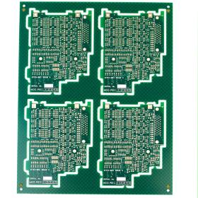
PCB depanelization is a process step in the production of large-scale assembly of electronics. To increase the throughput of printed circuit board (PCB) and surface mount (SMT) production lines, printed circuit boards are often designed to consist of many smaller individual printed circuit boards that will be used in the final product. This PCB cluster is called a panel or multi-block. The large panel is broken or "depanellated" as a process step - depending on the product, this can be right after the SMT process, after the in-circuit test (ICT), after soldering through-hole components, and even just before the final assembly of the PCBA in the enclosure.