
XIAMEN INNOVACERA ADVANCED MATERIALS CO., LTD
China

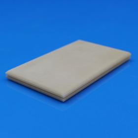
Product Name:Aluminum Nitride Ceramic Substrate, AlN Ceramic Sheet Application:Often used in electrical and electronic fields requiring heat conduction, heat dissipation, insulation, high temperature resistance,high voltage breakdown resistance, high thermal conductivity, good stability. Product specifications: Conventional models are TO-220, 247, 264, 3P Range thickness: 0.25mm, 0.385mm, 0.5mm, 0.635mm, 0.8mm, 1mm, 1.5mm, 2mm, 3mm Product Advantages: Aluminum nitride ceramics have excellent thermal conductivity (7-10 times of alumina ceramics),low dielectric constant and dielectric loss, reliable insulation performance, excellent mechanical properties, non-toxic, high temperature resistance, chemical corrosion resistance, and the thermal expansion coefficient of silicon is similar, as a new generation of ceramic materials, more and more by people Attention and attention.
XIAMEN INNOVACERA ADVANCED MATERIALS CO., LTD
China
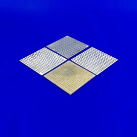
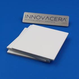
The Aluminum oxide (Al2o3) 96% ceramic plates are widely used in thick-film circuit of electronics industry. Large scale integrated circuit,power hytrid IC,semiconductor package,pieced -film reistor, network,resistor, focusing potentiometer etc.According to the demands of customers,our company can manufacture products of special types and specifications. Alumina ceramic substrate / plate specification: > 10x10x1mm, 20x20x2mm, 40x40x8mm, 100x60x8mm, 150x150x12.5mm, 200x200x25mm etc. > The thickness of ceramic plate ranges from 0.25 to 1.0mm Can be made according to your requirements.
XIAMEN INNOVACERA ADVANCED MATERIALS CO., LTD
China
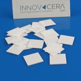
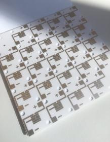
The Aluminum oxide (Al2o3 96%) ceramic substrate are widely used in thick-film circuit of electronics industry. Large scale integrated circuit,power hytrid IC,semiconductor package,pieced -film reistor, network,resistor, focusing potentiometer etc.According to the demands of customers,our company can manufacture products of special types and specifications. The Maximum dimension of ceramic plate is 138x138mm and the thickness of ceramic plate ranges from 0.25 to 1.0mm. Alumina Ceramic Substrate Features: > High reliablility and sfety; > High density and mechanical properties > High electrical and thermal loading perormances > Low dilelectic loss and other characteristics Alumina ceramic substrate / plate specification: 10x10x1mm, 20x20x2mm, 40x40x8mm, 100x60x8mm, 150x150x12.5mm, 200x200x25mm etc. Can be made according to your requirements.
XIAMEN INNOVACERA ADVANCED MATERIALS CO., LTD
China
No other oxide ceramic material collectively exhibits these highly desirable properties and characteristics. BeO ceramic conducts heat more quickly than virtually all metals with the exception of copper and silver. Beryllia exhibits extremely low dielectric loss characteristics, possesses high electrical resistivity, and offers excellent strength with high specific stiffness properties. BeO provides all the desirable physical and dielectric characteristics exhibited by an aluminum oxide or aluminum nitride, in addition, offers thermal conductivity ten times higher than alumina, and fifty percent higher than aluminum nitride, a dielectric constant that is lower than both alumina and aluminum nitride, and weight per given volume that is fully a quarter less than alumina, and nearly ten percent less than aluminum nitride. As a thermally conductive and electrically insulating material, its performance is exceeded only by that of the diamond.
XIAMEN INNOVACERA ADVANCED MATERIALS CO., LTD
China
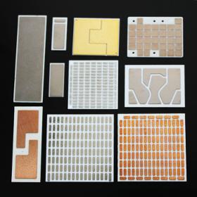
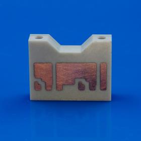
DBC (Direct Bonded Copper) tenique denotes a special process in which the copper foil and the al2o3 or AlN (one or both sides) are directly bonded under appropriate high temperature. The finished super-thin DBC substrate has excellent electrical isolation,high thermal conductivity, fine solderability and high bonding strength.It may be structured just lick PCB to get etched wiring and has high curreng loading capability .Therefore DBC ceramic substrates have become the base material of tuture for both the construction and the interconnection techniques of high power semiconductor electronic circuits and also have been the basis for "chip on boaed" technology which repre-sents the packaging trend in century. Specification >Metallization thickness: 25 ±10um >Nickel thickness:2~10um >Pin full strength: 4200kgf/cm2 avg. (at Φ3.0mm pin)
XIAMEN INNOVACERA ADVANCED MATERIALS CO., LTD
China
DBC ceramic substrate: Direct bonded copper (DBC) substrates are commonly used in power modules, because of their very good thermal conductivity. They are composed of a ceramic tile (commonly alumina) with a sheet of copper bonded to one or both sides by a high-temperature oxidation process (the copper and substrate are heated to a carefully controlled temperature in an atmosphere of nitrogen containing about 30 ppm of oxygen; under these conditions, a copper-oxygen eutectic forms which bonds successfully both to copper and the oxides used as substrates). The top copper layer can be preformed prior to firing or chemically etched using printed circuit board technology to form an electrical circuit, while the bottom copper layer is usually kept plain. The substrate is attached to a heat spreader by soldering the bottom copper layer to it. 1. Thickness of substrate can be thin: 0.25mm,0.28mm,0.45mm,0.5mm,0.635mm,1.0mm,1.5mm, 1.8mm,2.0mm 2.
XIAMEN INNOVACERA ADVANCED MATERIALS CO., LTD
China
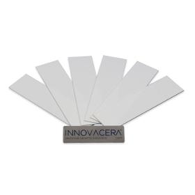
The Aluminum oxide (Al2o3 ) ceramic rectangle substrate is widely used in thick-film circuit of electronics industry. Large scale integrated circuit,power hytrid IC,semiconductor package,pieced -film reistor, network,resistor, focusing potentiometer etc.According to the demands of customers,our company can manufacture products of special types and specifications. Alumina ceramic substrate / plate specification: > 10x10x1mm, 20x20x2mm, 40x40x8mm, 100x60x8mm, 150x150x12.5mm, 200x200x25mm etc. > The thickness of ceramic plate ranges from 0.25 to 1.0mm Can be made according to your requirements.
XIAMEN INNOVACERA ADVANCED MATERIALS CO., LTD
China
The Aluminum oxide (Al2o396%) ceramic substrate are widely used in thick-film circuit of electronics industry. Large scale integrated circuit,power hytrid IC,semiconductor package,pieced -film reistor, network,resistor, focusing potentiometer etc.According to the demands of customers,our company can manufacture products of special types and specifications. The Maximum dimension of ceramic plate is 138x138mm and the thickness of ceramic plate ranges from 0.25 to 1.0mm. Features: 1.High reliablility and sfety; 2.High density and mechanical properties 3.High electrical and thermal loading perormances 4.Low dilelectic loss and other characteristics
XIAMEN INNOVACERA ADVANCED MATERIALS CO., LTD
China
AMB Ceramic Substrate is a method to realize the bonding of ceramic and metal by reacting a small amount of active elements Ti and Zr in filler metal with ceramics to form a reaction layer which can be wetted by liquid filler metal. Advantage: The combination is achieved by chemical reaction between ceramic and active metal solder paste at high temperature, so its bonding strength is higher and reliability is better. Disadvantage: The reliability of AMB process depends largely on the composition of active filler metal, brazing process, brazing layer structure and many other key factors。 Specification >Metallization thickness: 25 ±10um >Nickel thickness:2~10um; >Pin full strength: 4200kgf/cm2 avg. (at Φ3.0mm pin)
XIAMEN INNOVACERA ADVANCED MATERIALS CO., LTD
China
Aluminum nitride ceramics have excellent electrical and thermal properties, and are considered to be the most promising high thermal conductivity ceramic substrate materials. In order to seal the package structure, mount components and connect input and output terminals, the surface and interior of the aluminum nitride ceramic substrate need to be metallized. The reliability and performance of ceramic surface metallization have an important impact on the application of ceramic substrates, and firm bonding strength and excellent air tightness are the most basic requirements. Considering the heat dissipation of the substrate, it is also required to have high thermal conductivity at the interface between the metal and the ceramic. The metallization methods on the surface of aluminum nitride ceramics include: thin film method, thick film method, high melting point metallization method, electroless plating method, direct copper cladding method (DBC), etc.
XIAMEN INNOVACERA ADVANCED MATERIALS CO., LTD
China
DPC Ceramic Substrate Advantages: > In terms of shape processing, DPC ceramic substrate needs to be cut by laser, the traditional drilling and milling machine and punch machine can not be accurately processed, so the combination force and line width is also more fine. > The crystal performance of the metal is good; > The flatness is good; > The line is not easy to fall off; > The line position is more accurate, the line distance is smaller, reliable and stable, can be through the hole and other advantages.
XIAMEN INNOVACERA ADVANCED MATERIALS CO., LTD
China
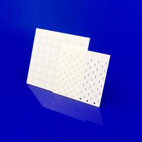
DPC (Direct Plated Copper) Mainly by evaporation,magnetron sputtering and other surface deposition process to carry on the substrate surface metallization,first under the condition of vacuum sputtering,titanium,and then is copper particles,the plating thickness,then finish making line with ordinary PCB craft,and then to plating/electroless deposition way to increase the thickness of the line, the preparation of DPC way contains vacuum coating,wet deposition,Exposure development, etching and other processes. Advantages: >In terms of shape processing, DPC ceramic plate needs to be cut by laser, the traditional drilling and milling machine and punch machine can not be accurately processed, so the combination force and line width is also more fine. >The crystal performance of the metal is good >The flatness is good >The line is not easy to fall off >The line position is more accurate,the line distance is smaller, reliable and stable, can be through the hole and other advantages.
EC PLAZA
South Korea
Ceracomb has its own technology to make and supply ceramic honeycombs and catalysts all together. we coat catalysts into the ceramic substrates for each purpose. Ceracomb supplies their catalysts for Automobiles and various industries. 1. DOC (Diesel Oxidation Catalyst) - DOC Catalyst efficiently oxidizes SOF among CO, HC, PM from diesel exhaust. 2. DPF (Diesel Particulate Filter)- DPF(Catalyzed DPF) oxidizes CO and HC which are not eliminated completely by DOC and help soot regeneration. 3. SCR (Selective Catalytic Reduction) - SCR Catalyst removes NOx from diesel vehicles. In the SCR process, NOx 4. AOC (Ammonia Oxidation Catalyst) - It is a catalyst to remove ammonia emitted from semiconductor processing and SCR post – processing devices. 5. TWC (Three Way Catalyst)- TWC converts HC, CO, NOx exhausted from gasoline vehicles into CO2, H2O, N2 [Application] - Replacement filter of DPF Converter - PM-NOx ATS - TWC Conveter for gasoline & LPG vehicles
XIAMEN INNOVACERA ADVANCED MATERIALS CO., LTD
China
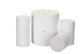
At present, conventional insulation materials have disadvantages such as low temperature resistance, low purity, gas release at high temperature, poor toughness, no insulation at high temperature, and easy to be corrosed. PBN insulation board can solve these problems. Main Features: 1. The maximum tolerance is 2300℃ in vacuum and 2700℃ in ammonia atmosphere; 2. High purity, high temperature does not release gas impurities (>99.99%); 3. Good toughness (hexagonal structure similar to graphite); 4. High temperature insulation (volume resistivity 3.11×10¹¹ ω •cm); 5. Intensification of inert, acid, alkali, salt and organic solvent corrosion; 6. Low thermal conductivity in the DIRECTION of C can block the downward conduction of heat and reduce heat loss PBN Plate Applications: For vacuum, high temperature, MBE equipment and other fields of insulation gasket, gasket, support, etc.
XIAMEN INNOVACERA ADVANCED MATERIALS CO., LTD
China
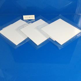
INNOVACERA® Hot Press Boron Nitride Sheet Thickness 2 mm, 3 Square in stock (25 x 25 mm, 50 x 50 mm, 200 mm x 240 mm), custom size is available. White in color. Hexagonal Boron Nitride has a microstructure similar to that of Graphite. In both materials this structure, made up of layers of tiny platelets, is responsible for excellent machinability and low-friction properties. we called hexagonal boron nitride (HBN) or white graphite. Features of Boron Nitride: 1.High thermal conductivity 2.Low thermal expansion 3.Good thermal shock resistance 4.High electrical resistance 5.Low dielectric constant and loss tangent 6.Microwave transparency 7.Non toxic 8.Easily machined — non abrasive and lubricious 9.Chemically inert 10.Not wet by most molten metals
XIAMEN INNOVACERA ADVANCED MATERIALS CO., LTD
China
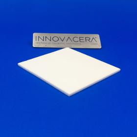
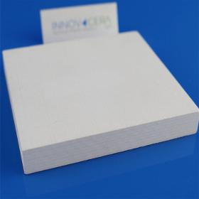
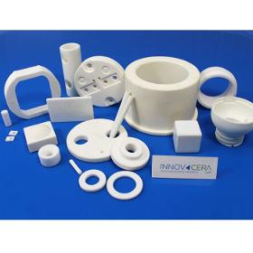
Aluminium Oxide, Al2O3 is a major engineering material. It offers a combination of good mechanical properties and electrical properties leading to a wide range of applications. Alumina can be produced in a range of purities with additives designed to enhance properties. A wide variety of ceramic processing methods can be applied including machining or net shape forming to produce a wide variety of sizes and shapes of component. In addition it can be readily joined to metals or other ceramics using metallising and brazing techniques. Alumina based ceramics are by far the largest range of advanced ceramics made by INNOVACERA. Due to the important combination of properties, we have thoroughly researched the behaviour and characteristics of our Alumina products to give you the best possible component. Typical Alumina characteristics include: Good strength and stiffness Good hardness and wear resistance Good corrosion resistance Good thermal stability Excellent dielectric properties
XIAMEN INNOVACERA ADVANCED MATERIALS CO., LTD
China
The Aluminum oxide (Al2o3) 96% ceramic plates are widely used in thick-film circuit of electronics industry. Large scale integrated circuit,power hytrid IC,semiconductor package,pieced -film reistor, network,resistor, focusing potentiometer etc.According to the demands of customers,our company can manufacture products of special types and specifications. Alumina ceramic substrate / plate specification: > 10x10x1mm, 20x20x2mm, 40x40x8mm, 100x60x8mm, 150x150x12.5mm, 200x200x25mm etc. > The thickness of ceramic plate ranges from 0.25 to 1.0mm Can be made according to your requirements.

Do you sell or make similar products?
Sign up to europages and have your products listed
XIAMEN INNOVACERA ADVANCED MATERIALS CO., LTD
China
The Aluminum oxide (Al2o3) 96% ceramic plates are widely used in thick-film circuit of electronics industry. Large scale integrated circuit,power hytrid IC,semiconductor package,pieced -film reistor, network,resistor, focusing potentiometer etc.According to the demands of customers,our company can manufacture products of special types and specifications. Alumina ceramic substrate / plate specification: > 10x10x1mm, 20x20x2mm, 40x40x8mm, 100x60x8mm, 150x150x12.5mm, 200x200x25mm etc. > The thickness of ceramic plate ranges from 0.25 to 1.0mm Can be made according to your requirements.
XIAMEN INNOVACERA ADVANCED MATERIALS CO., LTD
China
AMB (Active Metal Brazing) is for joining ceramics that are not wetted by 'conventional' brazes.By applying active metal like titanium to be added to the braze alloy, to achieve chemically reacts with the surface of the parent ceramic.Due to the coefficient of thermal expansion of Al2O3 (7.1 ppm/K), Si3N4 (2.6 ppm/K) and AlN (4.7 ppm/K) is close to that of silicon (4 ppm/K), Direct Bond Copper (DBC) and AMB are suitable substrates for robust packaging of bare dice since such assemblies.AMB is the promising thick film technology which can be applied to Power Electronics, Automotive Electronics, Home Appliances, Aerospace, Others. INNOVACERA provide DBC, DPC, and AMB technology for customized ceramic substrates, welcome to consult more.
COSMOCHROME LTD
Greece
It is suitable for fixing ceramic tiles on absorbent substrates like cement screeds and gypsum boards
3D-MICROMAC AG
Germany
3DMicromac‘s microSHAPE™ laser system is designed for the processing of large and flat substrates with high accuracy. The highly versatile system allows the combination of different laser processes in a single machine. In addition, it is capable of processing with multiple working heads – this parallel processing makes higher throughputs achievable. microSHAPE™ is an industry proven solution for all kinds of ablative and non-ablative processes. These include cutting, selective removal of thin films, and structuring processes like engraving and marking. The microSHAPE™ system is suitable for machining a variety of materials, e.g. glass, metals, polymer, ceramics, display stacks, and coated substrates. Free form cutting with extraordinary quality Damage free cutting edges Contactless processing enables minimal cost of ownership Cutting speed up to 1.5 m/sec Laser sources according to customer requirements Up to 3 independent beam paths
3D-MICROMAC AG
Germany
3DMicromac‘s microPRO™ is an adaptable laser micromachining system mainly used in industrial production. Its high versatility makes the system perfectly suited for industrial laser micromachining tasks such as laser structuring, cutting, and drilling applications. Furthermore, it is suitable for a variety of materials, e.g., metals, alloys, transparent and biological substrates, ceramics, and thin film compound systems. The microPRO™ is available with an automatic handling system for wafers, cassettes, trays, etc The microPRO™ enables the laser processing of various substrates. Due to the integration of different technology modules, the platform can be adapted to customers’ requirements. Configuration packages may include High speed cutting Drilling Engraving Structuring and modification Laser Lift Off (LLO) Cylindrical machining Customized solutions
MICROCERTEC
France
Laser ablation technology helps the engineer to develop circuit carriers which cannot be manufactured with chemical etching technology. This kind of product results from combining the technologies of precision-grinding of ceramics and laser ablation of metallised thin-film layers. We name this concept "three-dimensional interconnection circuit or CI3D". Principle The laser structuring consist to etch directly a metallization layer deposited on a ceramic carrier with a laser beam without using a mask. This is called laser micromachining or laser ablation - because metal is ablated. Laser ablation allows patterns to be etched directly on the ceramics substrate, very rapidly and beam displacements to be programmed limitless. Equipment Solid-state lasers are mostly used for micromachining applications because they feature precision, speed and selective etching. We currently use a Nd :YAG laser with 60 W output. It enables us to etch thin-film metallised layers with thickness of up...
MICROCERTEC
France
Microelectronic circuits continuously require new packaging technologies. Ceramic substrates are widely used in this field for their good dimension stability, high electrical insulation as well as their resistance to high temperature. But it is now possible to create microelectronic circuits on 3D carriers made with ceramics. This new type of component integrates electrical and mechanical functions on a same carrier, which gives a wider scope in terms of design and integration. Microcertec has developped a unique expertise to manufacture these ceramic 3D interconnection devices - CI3D - based upon high-precision ceramic grinding of a 3D carrier, thin-film metallizing and laser etching. These 3D interconnect carriers demonstrate the advantages of being made with advanced ceramics but they also offer miniaturization capabilities, enhanced reliability and more simple integration stages. In actual fact, the geometry of the carriers offers a 3D arrangement so that microelectronic...
DK CERAMIC CIRCUITS
Belgium
Ceramic prined circuit board feature many advantages over metal core and FR4 circuit boards as they combine excellent thermal characteristics with low a expansion. They are also suitable for multilayer applications, show lower deformation, warpage and operate under higher temperatures. Elite advanced technologies is your partner for ceramic substrates and circuit boards. Thanks to our large laser facilities and patented printing technology we are able to accomodate both very tight tolerances as well as high volume production at a high quality.
DK CERAMIC CIRCUITS
Belgium
LTCC (Low Temperature Co-fired Ceramic) is a multilayer capable substrate technology offering excellent RF and microwave performance characteristics. Thanks to its low sintering temperature (around 900°C) allows it to co-fire with highly conductive metals such as silver and gold. It is sometimes referred to as “glass ceramics” because glass is mixed in its main raw material, alumina. Elite Advanced Technologies is one of the few LTCC specialists globally that is producing its own green tape (base material low temperature co-fired ceramics). LTCC is best suited for applications that can take advantage of one or more of the following: Good electrical performance Dimensional and electrical stability under temperature, moisture and mechanical stress 3D capability curved, cavities, channels Effective thermal management with metal loaded vias (>100 W/MK) Hermeticity Matched TCE with semiconductors (Thermal Coefficient of Expansion) Multiple assembly and packaging solutions
Results for
Ceramic substrates - Import exportNumber of results
27 ProductsCompany type